Interfacial Chemical Vapor Deposition of Wrinkle-Free Bilayer Graphene on Dielectric Substrates

Abstract
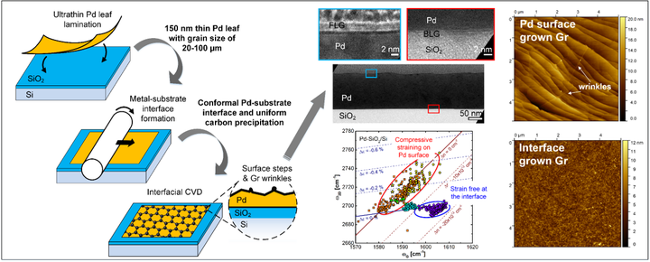
Wrinkles invariably form during graphene growth and post-growth transfer, limiting graphene films' large-scale uniformity for electronic applications. We report a transfer-free synthesis route for highly-uniform bilayer graphene directly on dielectric substrates—SiO2, sapphire, and MgO—by interfacial carbon precipitation. Ultrathin Pd leaves having a thickness of 150 nm and grain size up to 100 µm are laminated onto the target dielectric substrate, followed by annealing and press rolling to form a uniform Pd-substrate interface. Rapid heating in a hydrocarbon atmosphere causes carbon diffusion through the Pd layer; upon cooling, precipitation of carbon results in graphene growth at the Pd-substrate interface. The interface-grown graphene remains on the substrate after removing the Pd layer by wet etching. It exhibits sub-nm surface roughness without wrinkles or folds. Over 94% of the interface-grown area is dominated by bilayer graphene with low twist angles. In addition, the interface-grown graphene is nearly strain-free. From Raman characterization, an average long-range scattering mobility of ∼1000 cm2 V-1 s-1 was estimated for as-grown bilayer graphene on sapphire (0001) at room temperature. This technique shows promise to achieve device scale, ultra-uniform graphene fabrication directly on dielectric substrates, with the potential to accelerate graphene applications in electronics, photonics, and sensing.